Processing and Memory

Embedded Systems / Cyber-Physical System Fundamentals (ES/CPSF)

Peter Ulbrich

Winter Semester 2026/27
🚀 by Decker

Recap: Computation Under Constraints

From Chapter 02, we already know:

  • Work: a filter needs multiply–accumulate operations and data.
  • Meaning: word length, rounding, and saturation affect the result.
  • Constraints: deadlines, energy, and heat limit feasible execution.

Now we examine how operations and data accesses are organized inside the platform.

From Operations to Data Paths

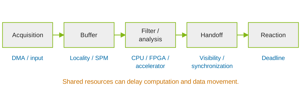
The familiar sensing pipeline needs both execution units and data delivery.
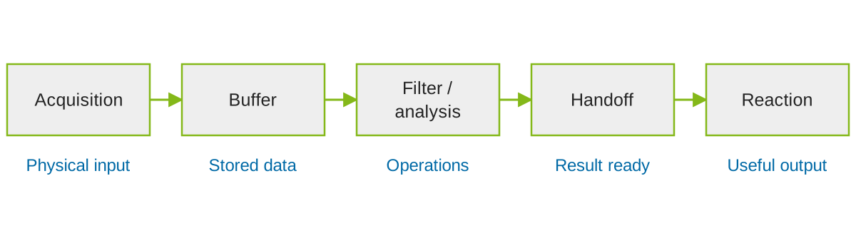
images/03-processing-memory/sensor-data-path.svg
Sensor pipeline from acquisition through a buffer and analysis to a reaction

Where are the operations executed? Where do their operands come from?

Useful processing includes movement, storage, computation, and timely handoff.

Learning Objectives

  • Execution: distinguish SIMD, VLIW/EPIC, multicore, and spatial hardware parallelism.
  • SoC organization: identify private/shared resources; distinguish heterogeneity from SMP/AMP.
  • Timing: distinguish intra-/inter-core effects and derive a contention bound in a stated model.
  • FPGA: explain LUTs, registers, configuration, and reconfiguration costs.
  • Memory: relate hierarchy, locality, working sets, and associativity to accesses.
  • Data delivery: compare cache/SPM, place data, and explain safe buffer handoff.

Chapter Map: Parallel Execution

Parallel ExecutionOperations, cores, and shared SoC resources
Reconfigurable HardwareLogic, configuration, and reuse over time
Memory OrganizationLocality, caches, scratchpads, and handoff

First, organize operations and instruction streams, then track contention for shared resources.

Forms of Parallel Execution

Form What proceeds concurrently? Small example
SIMD The same operation on several data elements Add four pixel values
VLIW / EPIC Explicitly scheduled independent operations Arithmetic and a load
Multicore Several instruction streams or tasks Control and image analysis
FPGA datapath Spatially instantiated operations and stages A pipelined filter

These mechanisms can coexist: each core may itself contain SIMD units.

Marwedel (2021), Sections 3.3.2–3.3.3. A conceptual comparison, not mutually exclusive product classes.

SIMD: One Operation, Several Data Elements
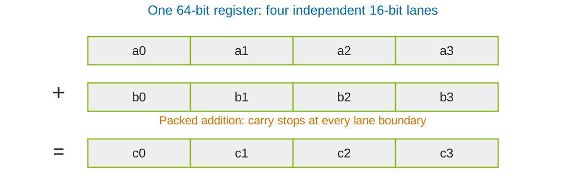
images/03-processing-memory/simd-packed-add.svg
Four 16-bit lanes in a 64-bit packed addition, with separate carry boundaries

SIMD: single instruction, multiple data. Narrow values share a wide register; examples include SSE and Arm Neon.

Vectorization must preserve overflow, rounding, and reduction semantics.

Marwedel (2021), Section 3.3.2, p.154, Fig.3.24. Lane count is an example, not a universal SIMD width.

VLIW and EPIC
images/03-processing-memory/vliw-packet.svg
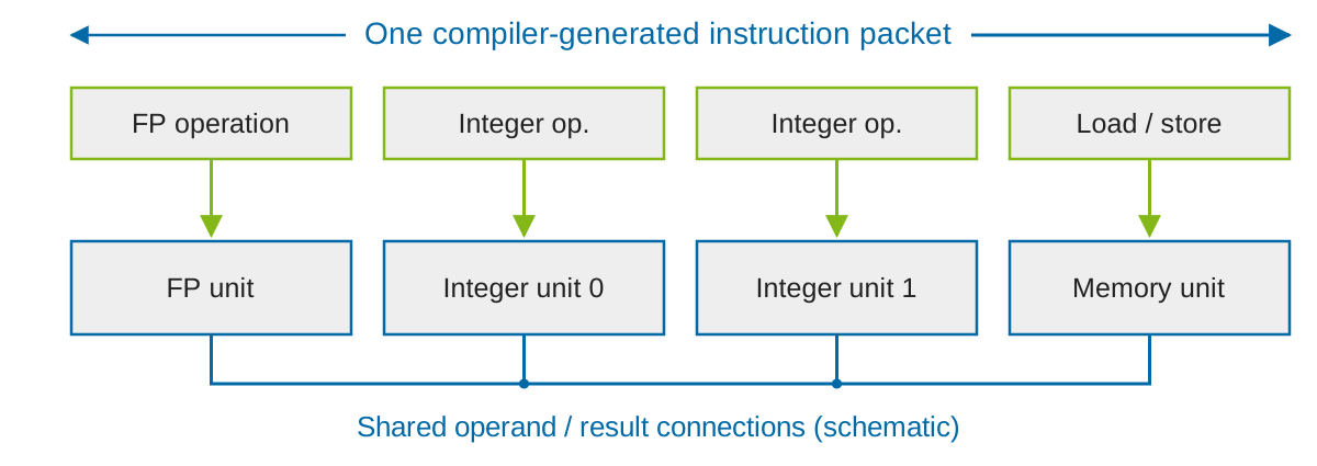
Span arrows group four instruction fields into one packet; four green arrows assign fields to functional units; a blue lower connection joins all units for schematic operand and result transfer
  • The compiler identifies independent operations and schedules resources.
  • Fixed packet fields may contain NOPs, increasing code size.
  • Explicit parallelism can also use more flexible packet encodings, as in TI C6xxx.

VLIW = very long instruction word; EPIC = explicitly parallel instruction set computer. Marwedel (2021), pp.155–156, Fig.3.25. Lower connection is schematic, not a specific register-file topology.

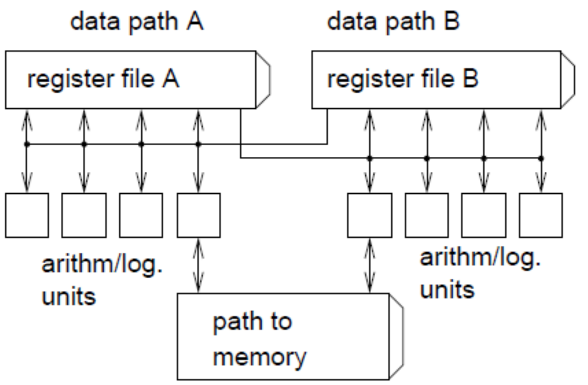
Supplying Operands: Partitioned Register Files

More operations per cycle require more simultaneous register accesses.

  • Extra ports increase area, energy, and access delay.
  • Partitioned files restrict connectivity.
  • Cross-path accesses remain limited.
images/03-processing-memory/partitioned-register-files.png
TI C6xxx datapaths A and B with partitioned register files and restricted cross paths

Parallel execution creates a data-supply problem inside the processor.

TI C6xxx diagram via Chen (2024); Marwedel (2021), p.156 and Section 3.4.3, p.170.

Small Controllers and Multicore Systems
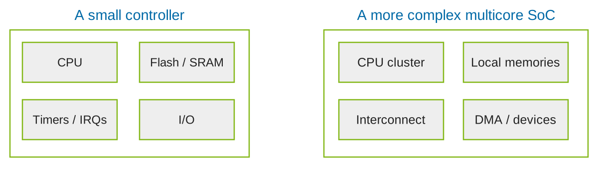
images/03-processing-memory/controller-components.svg
Functional comparison of a small controller and a more complex multicore SoC

Small controllers are often sufficient for sensing and control. Complexity follows the workload and system requirements.

A microcontroller can itself be a SoC and multicore. These labels describe different properties.

Generic functional diagrams.

Multicore: Private and Shared Resources
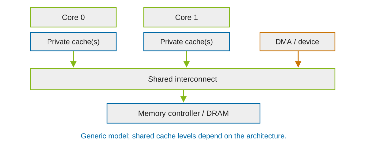
images/03-processing-memory/shared-soc-resources.svg
Generic two-core model with private caches, shared interconnect, DMA and common DRAM

More instruction streams share a finite memory and I/O infrastructure.

Generic teaching model after Marwedel (2021), pp.157–163. Private/shared cache levels and coherence depend on the actual platform.

Heterogeneous SoC: A Concrete Example
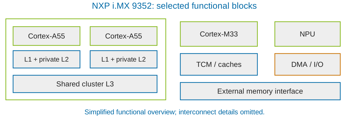
images/03-processing-memory/imx9352-overview.svg
Simplified i.MX9352 functional overview: two A55 cores, per-core L2, shared L3, M33, TCM, NPU and I/O

Possible roles: application processing, time-critical control, and specialized computation.

NXP IMX93IEC, Rev.8, July 2026, Table 1/Fig.2; simplified i.MX9352 overview. Features vary across derivatives. TCM = tightly coupled memory; NPU = neural processing unit.

SMP and AMP: Organizing the Cores
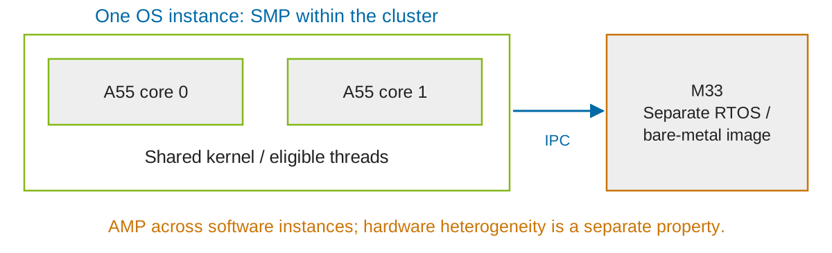
images/03-processing-memory/smp-amp.svg
An SMP A55 cluster and a separate M33 software instance cooperating through IPC

SMP: one OS instance manages eligible cores together. AMP: separate software instances cooperate explicitly.

Hardware heterogeneity and software organization are different distinctions.

SMP/AMP = symmetric/asymmetric multiprocessing; IPC = interprocessor communication. Marwedel (2021), pp.158–160; Zephyr SMP documentation. Illustrative OS allocation.

Parallelism, Latency, and Throughput
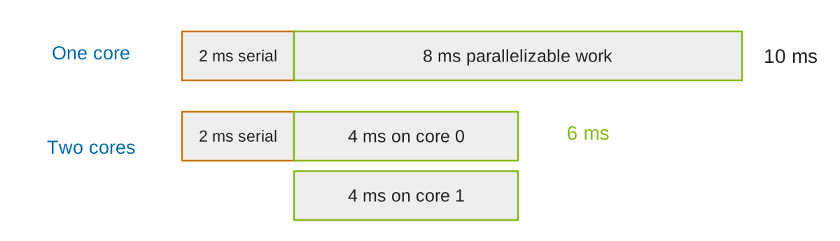
images/03-processing-memory/parallel-work-example.svg
Idealized fixed work taking ten milliseconds on one core and six on two cores

\[S(2)=\frac{10\,\mathrm{ms}}{2\,\mathrm{ms}+8\,\mathrm{ms}/2}\approx1.67\]

Latency: time for one result. Throughput: completed results per unit time.

Teaching model: 20% serial work; ideal split of the remainder; no communication, synchronization, or contention cost. This is not an end-to-end timing bound.

Timing Effects Within and Across Cores

Timing depends on hardware state and competing activity.

Timing source Mechanism Consequence
Core-local state Pipeline, predictor, cache / TLB history Different execution time even without another task
Intra-core task interference Another task runs on the same core and changes local state Additional cache / TLB reloads after resumption
Inter-core interference Other cores use shared caches, interconnect, or memory controller Extra lower-level requests and / or longer service

DMA and accelerators are additional requesters, even when CPU cores are dedicated.

Distinguish more requests from more waiting per request.

TLB: translation lookaside buffer. Maïza et al., timing-verification survey, 2019, Sections 1–3; EASA AMC 20-193, 2022, pp.6–8.

Memory Arbitration and Waiting-Time Bounds

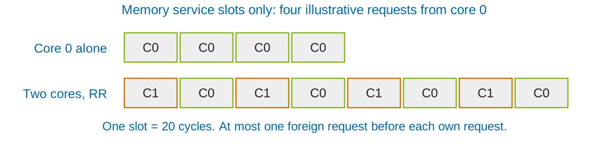
Task on core 0: \(C=1000\) compute cycles; \(n=20\) blocking requests, each requiring \(s=20\) service cycles.
images/03-processing-memory/arbitration-bound.svg
Four illustrative memory requests served alone or with one competing core under round-robin arbitration

\[T_{\mathrm{alone}}=C+ns=1000+20\cdot20=1400\ \text{cycles}\] \[W_{\max}\le s,\qquad T_{\mathrm{shared}}\le C+n(s+s)=1800\ \text{cycles}\]

Two requesters, one request per turn. Fixed request count; no computation–memory overlap or additional delays.

Own model: service time \(s=20\) cycles; two requesters; at most one foreign request ahead of each own request. Round-robin, one request per turn; no other delays, overlap, or change in request count. \(W_{\max}\): waiting before service. Diagram shows four of the twenty requests, excluding computation.

Moving Data: DMA and Buffer Traffic
images/03-processing-memory/shared-soc-dma.svg
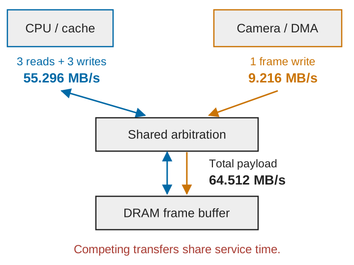
Three CPU read/write passes generate 55.296 MB/s and DMA frame writes 9.216 MB/s; shared arbitration serves their combined 64.512 MB/s payload traffic at the DRAM frame buffer

Example: 640 × 480 pixels, 1 B/pixel, 30 frames/s.

  • 307,200 B/frame = 300 KiB/frame.
  • Input payload: 9.216 MB/s.
  • One DMA write + three external read/write passes: 7 transfers/frame.
  • Modeled DRAM payload traffic: 64.512 MB/s.

DMA avoids a CPU copy loop, but still uses bandwidth and service time.

Own transfer-count model; MB = 10⁶ B, KiB = 1024 B. Assumes all seven transfers reach external memory; excludes protocol overhead and other traffic. DMA guide.

Chapter Map: Reconfigurable Hardware

Parallel ExecutionOperations, cores, and shared SoC resources
Reconfigurable HardwareLogic, configuration, and reuse over time
Memory OrganizationLocality, caches, scratchpads, and handoff

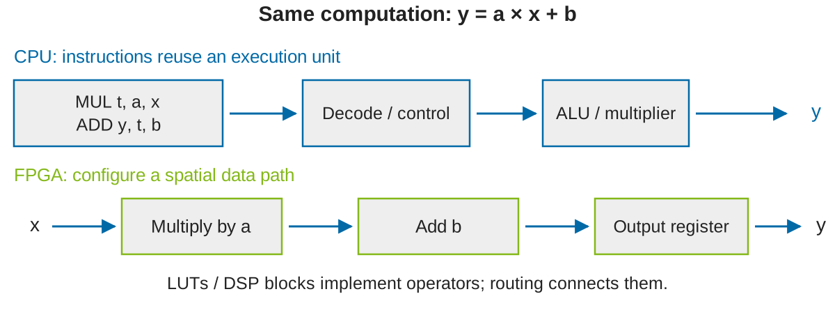
Software schedules operations on existing units. FPGA configuration defines the functions and connections of a datapath.

Reconfigurable Logic

images/03-processing-memory/configured-data-path.svg
The same expression y equals a times x plus b: CPU instruction control versus connected FPGA multiplier, adder and output register

A field-programmable gate array (FPGA) configures functions and connections to implement an application-specific data path.

Reconfigurability trades development cost, flexibility, performance, and energy efficiency.

Marwedel (2021), Section 3.3.3, p.165. The diagram is schematic; efficiency depends on workload and implementation.

FPGA Fabric: Logic Blocks and Routing
images/03-processing-memory/chen-fpga-routing.png
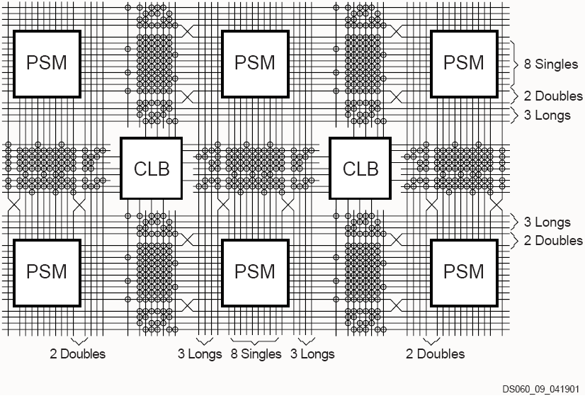
Original Xilinx fabric with CLBs, programmable switch matrices and routing channels of different lengths
  • CLB — Configurable Logic Block: LUTs, registers, and local multiplexers.
  • PSM — Programmable Switch Matrix: selects connections between routing wires.
  • Routing channels: carry signals between blocks; not every crossing is connected.

Dedicated blocks add RAM, DSP arithmetic, and I/O. A CPU may be a hard core in silicon or a soft core mapped to the fabric.

The bitstream configures both logic functions and connections.

Original Xilinx diagram, DS060_09_041901, via Chen (2024). Architecture-specific routing example, not a universal floorplan. Marwedel §3.3.3, pp.165–167.

LUTs, Registers, and Logic Blocks
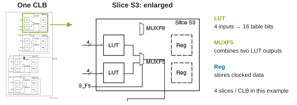
images/03-processing-memory/chen-clb-detail.svg
Original Xilinx CLB with four slices and a magnified slice S3 showing two four-input LUTs, multiplexers and registers; a separate legend names their functions

A look-up table (LUT) stores \(2^k\) output bits for \(k\) inputs. Multiplexers combine functions; registers hold working state.

Original Xilinx CLB image, UG002_c2_019_081600, via Chen (2024); one slice enlarged without changing its wiring. k: LUT input count; MUX: multiplexer; Reg: register. Four slices and four-input LUTs are specific to this example, not all FPGAs. Marwedel §3.3.3, pp.166–167.

Configuration Data and Working Data
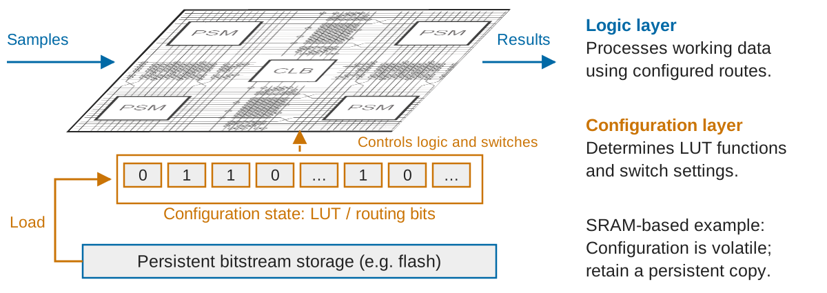
images/03-processing-memory/configuration-layers.svg
Original Chen logic plane with CLBs and switch matrices above configuration-state bits; a loading path supplies those bits from persistent bitstream storage, distinct from the blue sample flow

Example: inputs 01 yield 1 with XOR, but 0 with AND. Changing the LUT table changes the function, not the input samples.

Logic-plane image credited via Chen (2024) to Kalenteridis et al., Microprocessors and Microsystems, 2005. Configuration and storage layers reconstructed. SRAM-based example; bits and loading path are schematic. Marwedel §3.3.3, pp.165–167.

Reconfiguration at Run Time
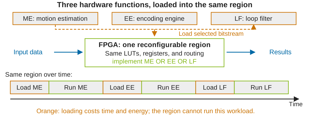
images/03-processing-memory/runtime-reconfiguration.svg
ME, EE and LF bitstreams configure the same central FPGA region in turn; a timeline distinguishes loading overhead from execution on that same region

Partial reconfiguration replaces one region while the static design remains configured. Switching also requires safe handoff of data and state.

Reuse over time saves resources only when reconfiguration costs fit the workload.

Video-encoder functions and partial-reconfiguration example after Chen (2024). Phase widths are schematic. Transfer time ≄ S/B: S is bitstream size [B], B configuration bandwidth [B/s]; switching may add drain/state-transfer time.

Chapter Map: Memory Organization

Parallel ExecutionOperations, cores, and shared SoC resources
Reconfigurable HardwareLogic, configuration, and reuse over time
Memory OrganizationLocality, caches, scratchpads, and handoff

The execution units are in place. Their operands still need capacity, bandwidth, and predictable access.

Memory Requirements and Technologies

Memory Organization

Technology Typical role Important trade-off
SRAM Registers, caches, local memory / SPM Fast access; limited density; volatile
DRAM Larger working memory Capacity; refresh and access-service costs
Flash Code, boot images, persistent data Persistence; erase/program constraints

Capacity, latency, bandwidth, access energy, cost, and predictable service can conflict.

Cache and scratchpad are organizations, not separate semiconductor technologies.

Marwedel (2021), Sections 3.4.1–3.4.2, pp.168–170. Qualitative comparison.

Why Small Memories Matter

images/03-processing-memory/memory-size-cost.png
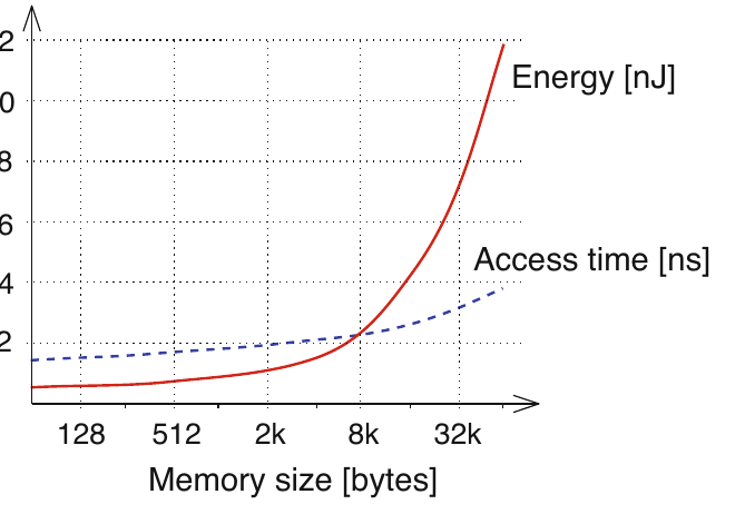
CACTI estimates of increasing memory access time and access energy with capacity

Larger arrays require longer wiring, decoding, and data paths.

  • Capacity can increase access time.
  • Access energy can grow more strongly.
  • Extra ports add a separate cost, as in register files.

Small is beautiful when frequently used information can stay close to computation.

Marwedel (2021), p.168, Fig.3.40, CACTI model; register-file detail Fig.3.42, p.170. Model-specific values, not current device specifications.

Memory Hierarchies
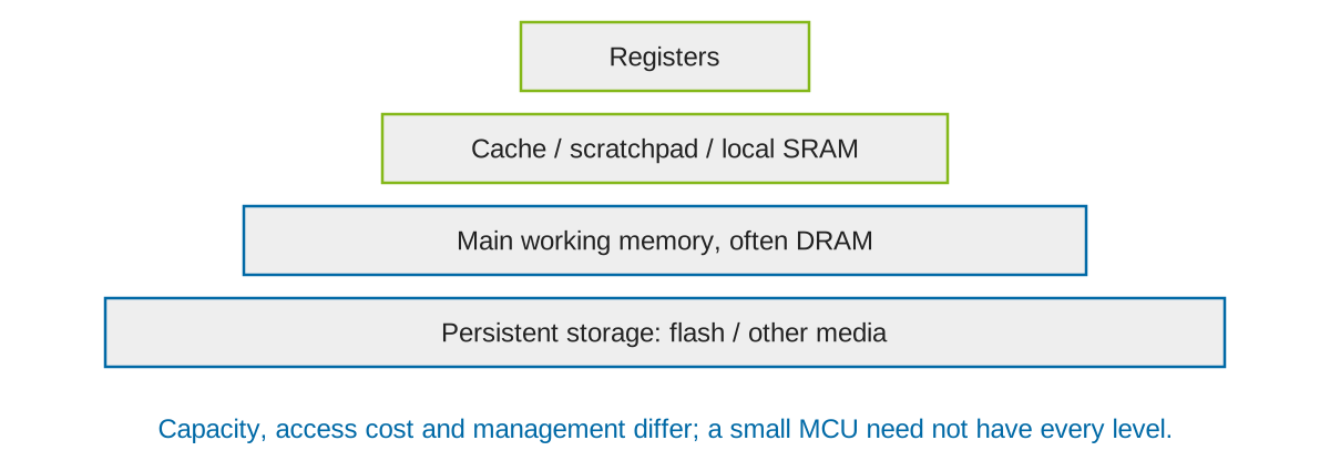
images/03-processing-memory/memory-hierarchy.svg
Hierarchy from processor registers through local SRAM, caches and main memory to persistent storage

Combine a small fast working set with larger storage; not every system needs every level.

Marwedel (2021), Section 3.4.2, pp.169–170. The historical memory-wall argument motivates hierarchy; throughput and latency remain separate constraints.

Locality and Working Sets

Property Access pattern Consequence
Temporal locality Reuse the same coefficients or samples Retain useful data near the core
Spatial locality Traverse adjacent array elements Use the rest of a fetched line
Working set Data and code active in a phase Capacity must fit the relevant phase

For a sliding filter, neighboring outputs reuse much of the same input window.

Memory behavior depends on layout and access order, not program size alone.

Marwedel (2021), Section 3.4.4, pp.170–172. Activates computer-organization knowledge.

Cache Lookup: Index, Tags, and Data

images/03-processing-memory/cache-lookup.svg
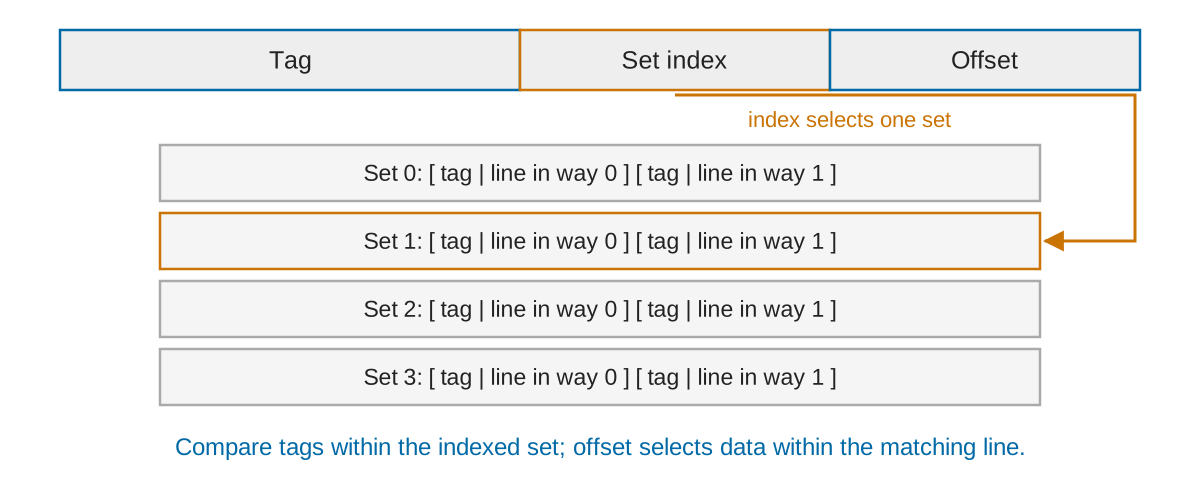
The index selects one cache set and tags are compared across that set’s ways; offset selects data

A hit uses a matching valid line. A miss requests a line from the next memory level.

Marwedel (2021), Section 3.4.4. Corrected reconstruction includes the line offset; it does not search all sets in parallel.

Mapping and Associativity: A Short Trace

Both caches: 64 B = four 16 B line slots. A: address 0, block 0. B: address 64, block 4.

Direct-mapped · 4 sets × 1 way
2-way · 2 sets × 2 ways
images/03-processing-memory/cache-associativity-step-1.svg
After reading A, both caches hold A in set 0; every other slot is empty
images/03-processing-memory/cache-associativity-step-2.svg
Reading B replaces A in direct-mapped set 0 despite three empty slots; the two-way cache keeps A and B together in set 0
images/03-processing-memory/cache-associativity-step-3.svg
Reading A again replaces B on the left, a miss; A is still present on the right, a hit

\(\text{block}=\lfloor\text{address}/16\rfloor\), \(\text{set}=\text{block}\bmod\text{number of sets}\). Blocks 0 and 4 select set 0 in both caches.

Three empty slots, but A must be reloaded: only its own set can hold it.

Own trace; Marwedel §3.4.4. Initially empty, read-only, no prefetch; capacity excludes metadata. A subsequent B also misses on the left and hits on the right.

Cache Interference After a Task Switch

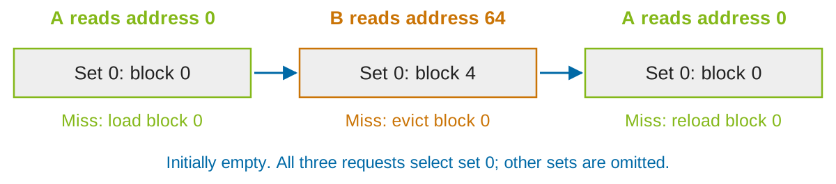
Direct-mapped cache: 64 B data, 16 B lines. Addresses 0 and 64 select set 0.
images/03-processing-memory/cache-task-interference.svg
Task B displaces task A’s line in set zero, so task A reloads it after resuming
Task A reads address 0 twice A’s first read A’s second read
A runs alone Miss Hit
B reads address 64 between A’s reads Miss Miss

One extra reload costs \(t_{\mathrm{miss}}-t_{\mathrm{hit}}\) in this blocking model, in addition to B’s CPU time.

Own trace: initially empty, read-only cache; no prefetch or overlap. \(t\): access latency. Intra-core example: B runs during A’s preemption. Inter-core analogue: conflicts in a shared cache, when requests reach it. Maïza et al., 2019, Section 1; Rouizi et al., ECRTS 2025, p.19:2.

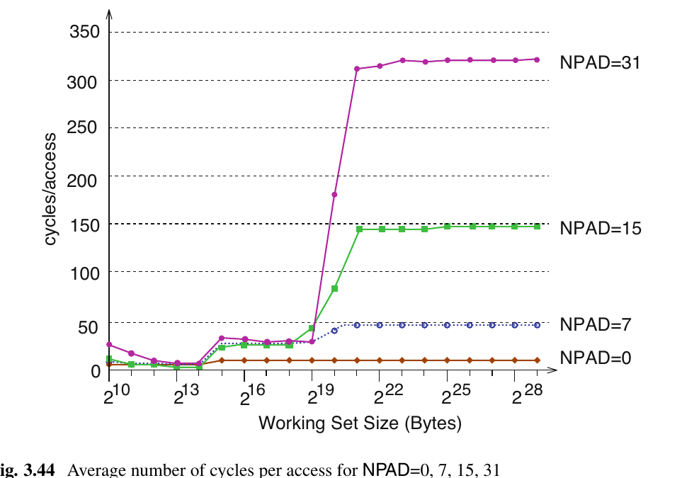
Working Sets Change Execution Time
images/03-processing-memory/cache-working-set.png
Measured average cycles per access versus working-set size, with padding-dependent behavior

Marwedel (2021), p.172, Fig.3.44, Drepper’s Pentium-4 experiment. NPAD: additional 64-bit words per list element. Mean cycles/access, not a WCET bound or a current benchmark.

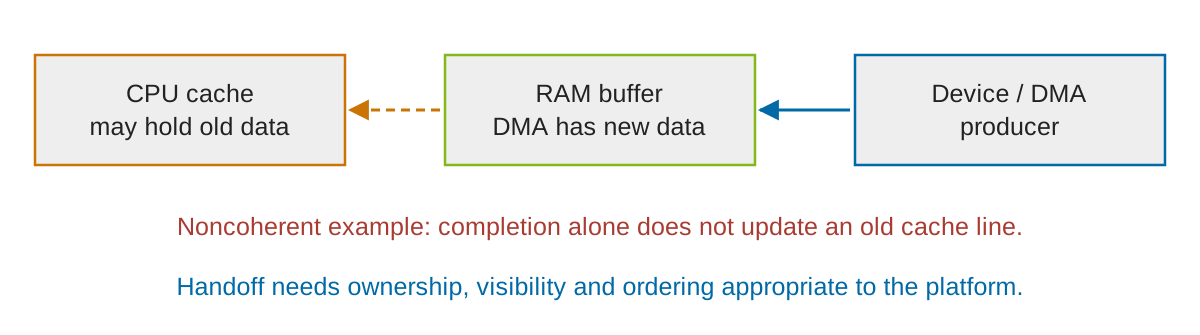
Coherence and DMA Handoffs
images/03-processing-memory/dma-handoff.svg
A generic noncoherent DMA producer updates RAM while a CPU cache may retain stale data
  • Coherence: how are copies of the same address kept compatible?
  • Ordering / synchronization: when may the receiver observe data and readiness?
  • Ownership: who may read or modify the buffer now?

Generic noncoherent case, not an assertion about the i.MX9352 path. Linux DMA guide; memory barriers, “Cache coherency vs DMA”.

Scratchpad Memories
images/03-processing-memory/scratchpad-address-map.svg
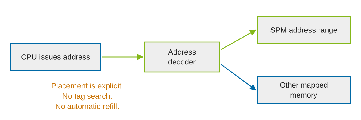
Address decoding selects a scratchpad address range or another mapped memory region

Software, compiler, and linker place selected code or data into the SPM address range.

SPM access is explicitly addressed; it has no cache-style automatic replacement or refill.

Marwedel (2021), Section 3.4.5, pp.172–173, Fig.3.45. Concrete TCM interfaces and accessibility are device-specific.

Cache and Scratchpad: Costs and Control
images/03-processing-memory/cache-spm-access-energy.png
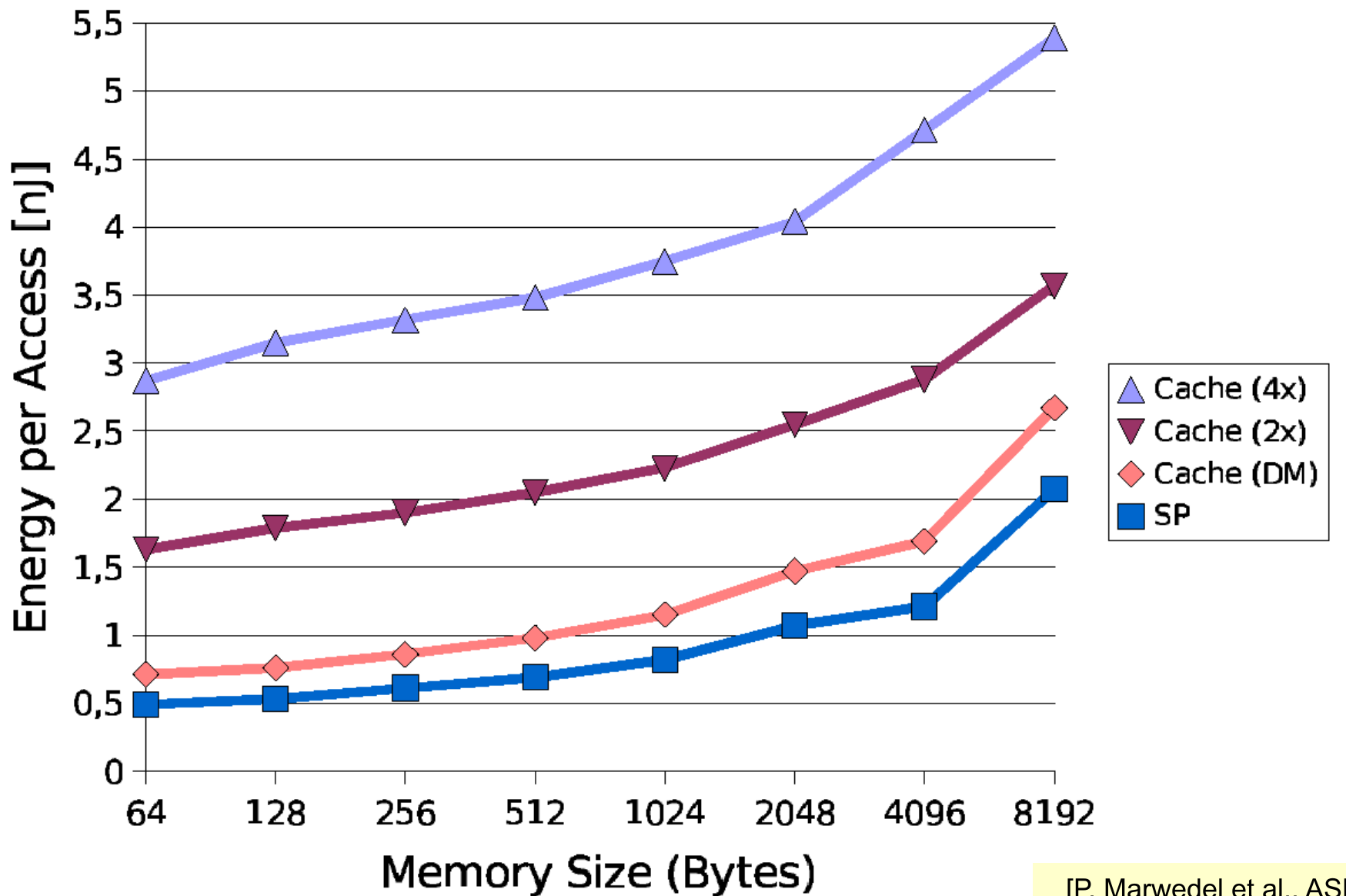
Access energy for direct-mapped, two-way and four-way caches compared with scratchpad in a 2004 study
  • Cache: hardware-managed residency; tags and replacement.
  • SPM: explicit placement; simple address selection.
  • Whole-system cost: include slow-memory accesses, transfers, and execution time.

More control can improve predictability, but placement quality still matters.

P. Marwedel et al., ASPDAC 2004, via Chen (2024). Technology-specific access-energy comparison; 2x/4x denote ways. See also Marwedel (2021), Fig.3.46, p.173.

Placing Data in a Scratchpad

8 KiB SPM. Each replaced main-memory access saves 3 nJ in this model.

Object Size Accesses / run Saving if placed
A 4 KiB 1000 3000 nJ
B 4 KiB 100 300 nJ
C 8 KiB 1500 4500 nJ

Feasible choices: none, A, B, A+B, or C. A+B: 3300 nJ; C: 4500 nJ.

Choose C in this model. Access frequency must be considered together with object size and total benefit.

Own static-placement example after Marwedel (2021), Sections 3.4.5 and 7.3.3. Ignores initial loading and any cache; real transfer costs require separate accounting.

Temporal Isolation: Which Channel Is Controlled?

Mechanism What it controls What still needs analysis
Dedicated core CPU-time sharing with other tasks Shared cache, interconnect, memory, DMA
Cache partitioning Cross-partition capacity evictions Shared cache service and downstream memory traffic
Memory-access budget \(Q\) per \(P\) Request volume over a regulation window Bursts, enforcement delay, unregulated requesters
Local SPM / TCM placement Selected accesses avoid a shared path Remaining code, buffers, transfers, and actual local-memory connectivity

A timing argument must cover all relevant interference channels and the service they receive.

\(Q\): permitted memory transactions; \(P\): regulation interval. TCM: tightly coupled memory. MaĂŻza et al., 2019; Zuepke et al., MemPol, 2024. Model limits: Rouizi et al., 2025.

Memory Regulation: Time Scale Matters

images/03-processing-memory/mempol-regulation-2024.png
MemPol and MemGuard regulate a worst-case reader at fifty percent sustainable bandwidth on ZCU102, with different short-term burst patterns

Same target, different bursts: MemGuard uses a 1 ms period; MemPol polls every 6.25 ”s with a 50 ”s sliding window. Similar long-term bandwidth does not establish the same per-request delay bound.

Zuepke, Bastoni, Chen, Caccamo, Mancuso. MemPol, Real-Time Systems 60, 2024, Fig.3, p.376. Paper, CC BY 4.0. Figure cropped from the original PDF; axes, legend, and curves unchanged. Platform: ZCU102; target: 50% sustainable bandwidth. Measurements, not a WCET proof.

Following the Complete Data Path

images/03-processing-memory/sensor-data-path-complete.svg
Sensor data path annotated with DMA, memory locality, computation, handoff and deadline constraints

Which bottlenecks or correctness problems would more CPU cores alone fail to remove?

Trace operations, transfers, handoffs, and shared resources before claiming a timing result.

Chapter Summary

  • Parallelism: data lanes, explicit operations, cores, and spatial datapaths can coexist.
  • Timing: other tasks can add cache misses or increase shared-resource waiting; isolation must cover both.
  • FPGAs: configuration defines functions and connections; changing it costs time and energy.
  • Memory: locality, working set, and mapping shape access behavior.
  • Handoff and placement: data must be available, correctly published, and stored in suitable regions.

Hardware organization connects functional correctness, resource cost, and timing.

Self Check

Q1 · Execution
How can SIMD and multicore execution coexist?

Q2 · SoC
Which resources are private, shared, or independently managed?

Q3 · Timing
Derive the 1800-cycle bound. What changes with a third requester? Which channel survives cache partitioning?

Q4 · FPGA
What changes during reconfiguration? What remains ordinary working data?

Q5 · Cache
Trace A–B–A–B in both caches. Why can B add a miss to A without changing A’s own reads?

Q6 · Data delivery
Which object belongs in the 8 KiB SPM? Is DMA completion enough for safe access?

References

Reading in Marwedel

Fourth edition (2021)

  • SIMD, VLIW, register ports → §3.3.2, pp.154–156
  • Multicore and MPSoCs → §3.3.2, pp.157–165
  • Reconfigurable logic → §3.3.3
  • Memory organization → §3.4.1–3.4.5
  • SPM placement, further reading → §7.3.3
  • Timing analysis, later → §5.2.2

Technical documentation: NXP i.MX 93, Rev.8, 2026; Linux DMA guide and memory barriers.

Bibliography

  1. P. Marwedel. Embedded System Design. 4th ed., Springer, 2021. Open-access book.
  2. J.-J. Chen, G. von der BrĂŒggen. Processing (Part II) / Memory. Lecture slides, 2024, based on P. Marwedel.
  3. C. MaĂŻza et al. A Survey of Timing Verification Techniques for Multi-Core Real-Time Systems. ACM Computing Surveys, 2019. DOI.
  4. A. Zuepke et al. MemPol: polling-based microsecond-scale per-core memory bandwidth regulation. Real-Time Systems, 2024. DOI.
  5. L. Rouizi et al. Revisiting Timing Anomalies in Predictable In-Order Pipelines. ECRTS, 2025. DOI.
  6. V. Kalenteridis et al. A complete platform and toolset for system implementation on fine-grain reconfigurable hardware. Microprocessors and Microsystems 29(6), 247–259, 2005. DOI.